Computer chips are the basis for nearly every electronic device produced today. The tiny circuits that compose them can carry out computations, make decisions, and store information. Sustained research in new microchips for efficient computing and advanced artificial intelligence (AI) has been recognized as critical for U.S. strategic interests and Department of Defense priorities by former and current administrations to keep up with performance demands.
AI models are an area where innovation is particularly important as companies are looking to increase their model’s performance, which in turn requires more computational power that has to be delivered by the hardware. Devices inspired by the brain’s neurons and synapses promise high-performance accelerator chips that meet the small size/weight and ultra-low power hardware needs for the training and inference of AI models.
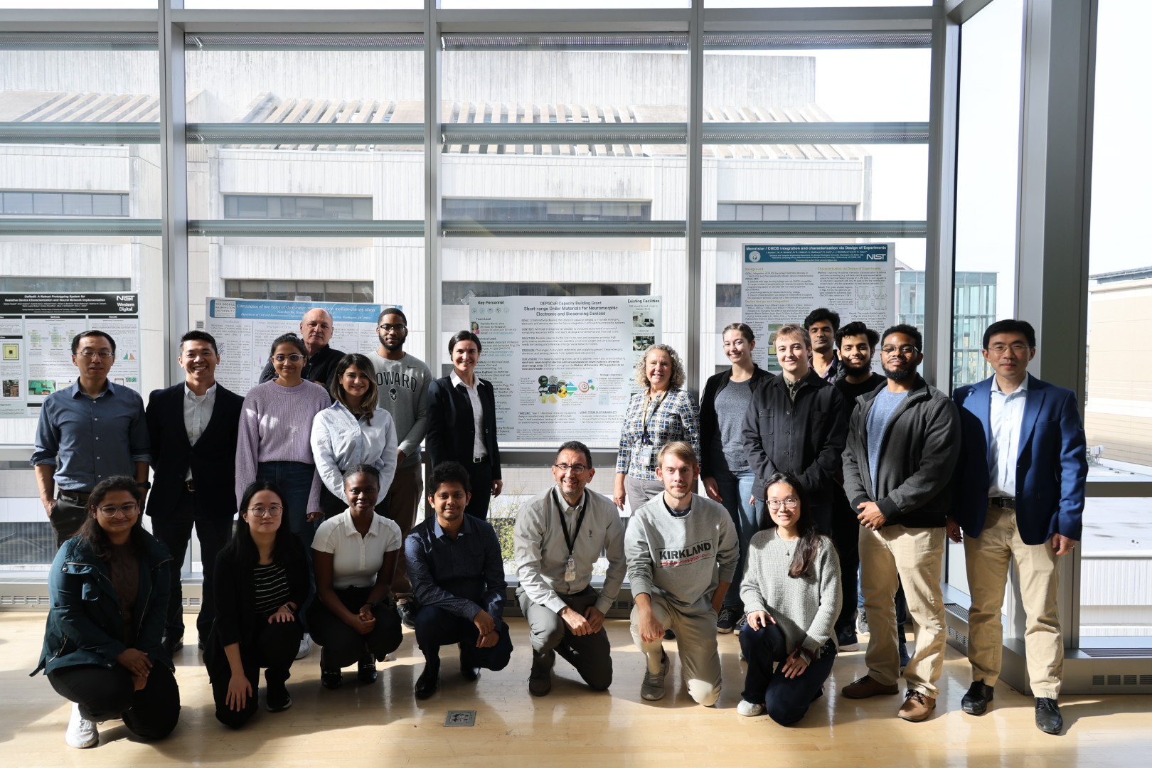
However, these emerging electronic and sensing devices present challenges in low yield, poor uniformity, and scalability, which prevent them from system-level adoption. Researchers from GW’s School of Engineering & Applied Science (GW Engineering) are leading a strong team of scientists from the Washington D.C.-Metro area, including from Georgetown University, Catholic University of America, Howard University, and Gallaudet University, to address this issue.
The $1M Defense Established Program to Stimulate Competitive Research (DEPSCoR) capacity-building grant from the Department of Defense, “Short-range Order Materials for Neuromorphic Electronic and Biosensing Devices,” supports this team in collaboratively developing the regional research capacity needed to create new types of devices for next-generation computing. In particular, they are focusing on emerging electronic and sensing devices for future integration in brain-inspired, also known as neuromorphic, computing systems.
“This DEPSCoR capacity-building project is allowing us to purchase a piece of unique sputtering equipment and to investigate new types of neuromorphic devices for computing and sensing based on novel materials driven by short-range order. This interdisciplinary work, as well as the proposed research and facility capacity building, is very exciting for me and my collaborators at GW and neighboring universities,” said Gina Adam, assistant professor of electrical and computer engineering at GW and technical lead on the project.
Adam is working closely with team lead Pamela Norris, GW’s vice provost for research and professor of mechanical and aerospace engineering, who stated, “This project brings a unique capability to our device growth, characterization, and design capabilities. The sputtering system is a tool I wish I had access to as a researcher myself designing tailored thermal conductivity in thin film materials.”
Additional collaborators from GW Engineering include co-technical leads Tianshu Li, a professor of civil and environmental engineering, and Mona Zaghloul, a professor of electrical and computer engineering. Can Korman, professor of electrical and computer engineering, Anastas Propratiloff, director of the GW Nanofabrication and Imaging Center (GWNIC), and Yigal Lilach, senior cleanroom specialist in the GWNIC, are supporting the equipment installation and research efforts.
The first thrust of the project is investigating novel short-range order materials to develop new materials for neuromorphic computing. To illustrate how the research team is working to accomplish this while also tackling the challenge of predicting complex material characteristics, Li gave the example of the movie Iron Man. In the film, there is a scene where Iron Man is building his armor and picks elements from the periodic table and combines them to generate properties, which he then decides if that is what he wants or not. According to Li, they are doing the same thing but in simulation. Now, the novel sputtering system allows the researchers to physically deposit these materials in a way that supports their integration in devices and systems.
“This research topic examines the most promising materials for neuromorphic computing systems. Along the way, it offers resources to build infrastructure, like the sputtering system we’re discussing, that allows us to deposit nanostructured materials with an extremely high level of atomic control so we can design materials with technological insight and test out their properties,” said Kai Liu, a professor of physics and project collaborator at Georgetown University.
For example, Li is utilizing his expertise in modeling short-range order materials to make predictions on how materials will behave and what kinds of properties will be created for a given combination of elements. That information is then passed to Adam and Liu, who synthesize those materials using the sputtering system for their respective devices. Once they make the material, it is characterized to give Li feedback on the experimental material properties, forming a feedback loop. The hope is to eventually reach convergence and discover new materials, which the team will use to develop analog neuromorphic devices and biosensing devices for neuromorphic sensory systems.
“The university has made a huge investment in our Nanofabrication and Imaging Center. I’m very glad this project is leveraging that investment and helping it grow. I think that’s the most significant aspect because it shows if the university makes investments in these types of facilities, then we will start getting the returns. The returns are the growth in these types of state-of-the-art facilities and capabilities at GW; that’s number one. Number two is that it opens doors to us we originally could not have had; specifically, it enables us to collaborate and lead innovative research projects with other universities in the area,” Korman stated.
Strengthening collaborations is a strategic objective of this capacity-building project. Regarding the benefits of this collaboration, Robert Coleman, a third-year Ph.D. candidate at Howard University in Eric Seabron’s group, said, “Every university and group represented here has different expertise, equipment, and resources at their disposal that the others might not necessarily have or would have to jump through many hoops to get to or travel very far to. By having this collaboration, we’re not only sharing information but resources as well.”
“The opportunity provided by this DEPSCoR capacity-building grant to further strengthen relationships with other district universities is very exciting. We have a great diversity of universities in the district and, together, we can have a much greater impact,” said Norris.
This capacity-building project also targets investments in workforce development across the educational pipeline. The team is developing new undergraduate courses in microelectronics and nanofabrication and providing support to students pursuing research and internship opportunities in this area. Moreover, outreach events with other local universities and high schools are being organized with a focus on hands-on training in nanotechnology for female students, underrepresented minorities, and students with disabilities.
For example, Gallaudet University supports deaf and hard-of-hearing students, getting them engaged in research and interested in careers in science, technology, engineering, and mathematics. In this project, the team is developing accessible education modules using virtual reality simulations to support these efforts. At the same time, the hearing members will benefit from interactions with deaf and hard-of-hearing participants and collaborators leading to a more diverse and culturally enriched work environment.
“We will use these educational modules as a way for these students to go through the semiconductor manufacturing procedures and different kinds of cleanroom experiments and operations virtually. Eventually, they will come to GW and use the facilities in the Nanofabrication and Imaging Center,” said Paul Sabila, a professor of chemistry at Gallaudet University.
Students from all involved universities are contributing to varying aspects of this project. By supporting research in these hot topic areas while still in school, these students are gaining valuable experience before they enter industry or academia. Under the guidance of Dr. Adam, first-year Ph.D. candidate Shweta Joshi is working on high-entropy oxides, which she says are showing promising results to be used in more reliable memristor devices, suitable for system-level adoption.
“During my Ph.D., I aim to explore their unique properties at the material and device levels. After graduation, I hope to join either industry or academia, leveraging this project’s experience in neuromorphic devices and materials research. It would be amazing to contribute to this research that will hopefully make memristor devices integrated on consumer chips a reality in a few years,” said Joshi.
“For students, this project brings a unique experience to make them more competitive. That was the foundation for building the Nanofabrication and Imaging Center. It is not just for research, but an important mission of this facility is to give students unique hands-on experiences,” Propratiloff stated.
Ultimately, this capacity-building project is allowing the team to address the current and emerging issues in electronic and sensing devices while increasing collaborative research in the region, creating a unique infrastructure in the Mid-Atlantic, and developing a diverse workforce trained in materials and devices.
“For D.C., this is not only an opportunity for faculty to push forward the next-generation solution for electronic and material science, but also for students to get educational training and practical research experience in terms of what will happen in the next five to ten years,” Hieu Bui, assistant professor of electrical engineering and computer science at Catholic University of America, emphasized.
The overarching vision is to use this opportunity as a stepping-stone for larger initiatives and to strengthen D.C.’s position as an innovation leader in energy-efficient neuromorphic systems. There is a critical need to maintain leadership in the U.S. semiconductor and nanotechnology industry, particularly given the rise in AI. Given the CHIPS Act efforts, it is of utmost importance for the D.C. universities to have a strong voice in this interdisciplinary area of neuro-inspired chip technologies, attract the necessary resources, and support research and education efforts. This project targets significant long-term growth in research collaborations across the involved institutions and the material and device technology transfer to companies and Department of Defense labs.
“This DEPSCoR capacity-building grant positions GW Engineering well to establish a D.C. consortium that supports this vision,” said Adam.
This material is based upon work supported by the Air Force Office of Scientific Research under award number FA9550-23-1-0497.


